 Grow Career Publication
1.Intrinsic Semiconductor
- Books Name
- Physics Book Part l and ll
- Publication
- Grow Career Publication
- Course
- CBSE Class 12
- Subject
- Physics
Chapter 14: Semiconductors Electronics
Intrinsic Semiconductor
CLASSIFICATION OF METALS, CONDUCTORS AND SEMICONDUCTORS
Metals:
They possess very low resistivity (or high conductivity).
![]()
Semiconductors:
They have resistivity or conductivity intermediate to metals and insulators.
![]()
Insulators:
They have high resistivity (or low conductivity).
![]()
The values of ρ and σ have given above are indicative of the magnitude and could well go outside the ranges as well.
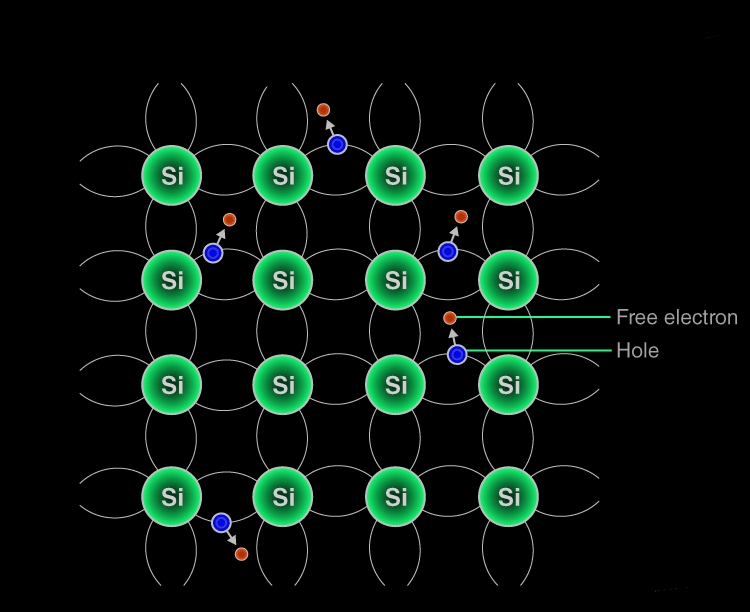
Intrinsic Semiconductors
Semiconductors that are chemically pure, in other words, free from impurities are termed as intrinsic semiconductors. The number of holes and electrons is therefore determined by the properties of the material itself instead of the impurities. In intrinsic semiconductors, the number of excited electrons is equal to the number of holes; n = p.
Working Mechanism of Intrinsic Semiconductors
Electronic Configuration of Silicon and Germanium
Silicon 1s2 2s22p6 3s2 3p2
Germanium 1s2 2s2 2p6 3s2 3p6 4s2 3d10 4p2
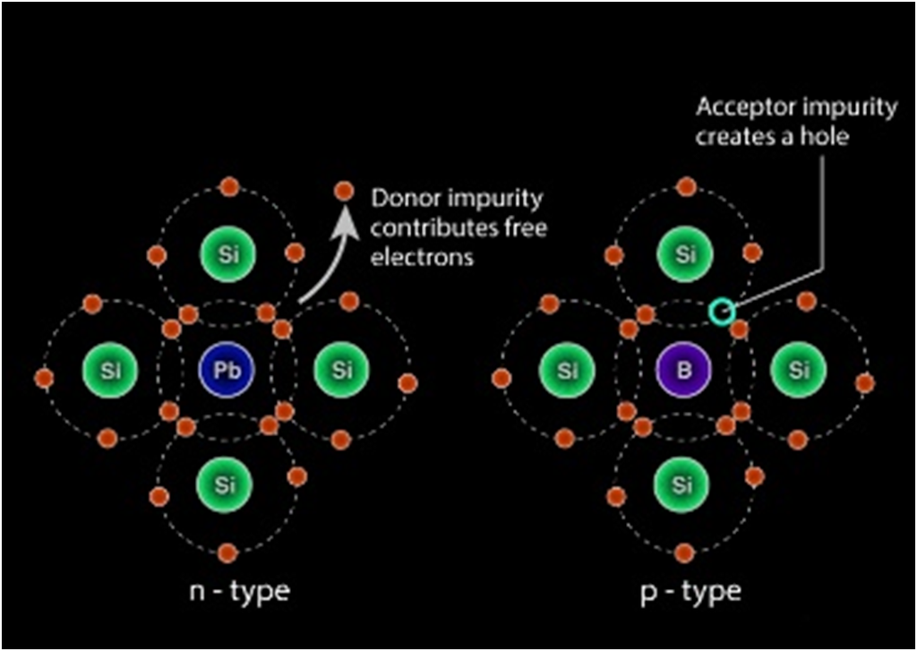
EXTRINSIC SEMICONDUCTOR
n-type semiconductors
When a tetravalent atom such as Si or Ge is doped with a pentavalent atom, it occupies the position of an atom in the crystal lattice of the Si atom. The four of the electrons of the pentavalent atom bonds with the four neighboring silicon atoms and the fifth one remains weakly bound to the parent atom. As a result of this, the ionization energy required to set the fifth electron free is very less and the electrons become free to move in the lattice of the semiconductor. Such semiconductors are termed as n-type semiconductors.
2. p-n Junction and diode
- Books Name
- Physics Book Part l and ll
- Publication
- Grow Career Publication
- Course
- CBSE Class 12
- Subject
- Physics
P-n Junction and diode
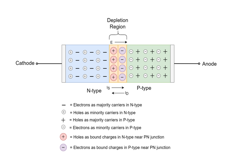
p-n JUNCTION
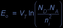
The total charge on each side of a PN Junction must be equal and opposite to maintain a neutral charge condition around the junction. If the depletion layer region has a distance D, it therefore must therefore penetrate into the silicon by a distance of Dp for the positive side, and a distance of Dn for the negative side giving a relationship between the two of:
Dp*NA = Dn*ND
in order to maintain charge neutrality also called equilibrium.
SEMICONDUCTOR DIODE
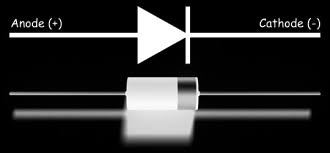
A Semiconductor Diode is a p-n junction that has metallic contacts at both of its ends in order to apply external voltage. It is a p-n junction diode. It has the ability to conduct current in only one direction.
p-n junction diode under forward bias
When an external voltage V is applied across a semiconductor diode such That p-side is connected to the positive terminal of the battery and n-side To the negative terminal.
p-n junction diode under reverse bias
When an external voltage (V ) is applied across the diode such That n-side is positive and p-side is negative, it is said to be Reverse biased.
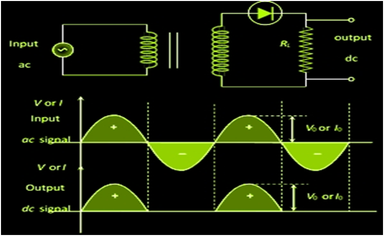
APPLICATION OF JUNCTION DIODE AS A RECTIFIER
In a half-wave rectifier, one half of each a.c input cycle is rectified. When the p-n junction diode is forward biased, it gives little resistance and when it is reversing biased it provides high resistance. During one-half cycles, the diode is forward biased when the input voltage is applied and in the opposite half cycle, it is reverse biased. In the Full-wave rectifier circuits are used for producing an output voltage or output current which is purely DC. The main advantage of a full-wave rectifier over half-wave rectifier is that such as the average output voltage is higher in full-wave rectifier, there is less ripple produced in full-wave rectifier
SPECIAL PURPOSE p-n JUNCTION DIODES
Zener diode
It is a special purpose diode, named after the inventor C. Zener It is designed to operate under reverse bias in the breakdown region
The symbol for Zener diode is
Fabrication – It has heavily doped p- side and n-side. Due to this, the depletion region formed is very thin about < 10-6. . Hence, the field at the junction is extremely high about -5 * 106 V/m for a small reverse bias voltage of 5 Volts
Light emitting diode
It is a heavily doped p-n junction which under forward bias emits Spontaneous radiation. The diode is encapsulated with a ttransparen Cover so that emitted light can come out.The V-I characteristics of a LED is similar to that of a Si junction Diode. But the threshold voltages are much higher and slightly different For each colour. The reverse breakdown voltages of LEDs are very low, Typically around 5V. So care should be taken that high reverse voltages Do not appear across them.
Solar cell
A solar cell is basically a p-n junction which Generates emf when solar radiation falls on the p-n junction. It works on the same principle (photovoltaic effect) as the photodiode, except that No external bias is applied and the junction area Is kept much larger for solar radiation to be Incident because we are interested in more power.
JUNCTION TRANSISTOR
n-p-n transistor: Here two segments of n-type semiconductor (emitter and collector) are separated by a segment of p-type Semiconductor (base).
P-n-p transistor: Here two segments of p-type semiconductor (termed as emitter and collector) are separated by a segment of n-type semiconductor (termed as base).
The schematic representations of an n-p-n and a p-n-p Configuration.
DIGITAL ELECTRONICS AND LOGIC GATES
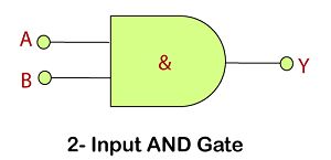
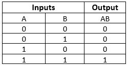
AND Gate
This gate works in the same way as the logical operator "AND". The AND gate is a circuit that performs the AND operation of the inputs. This gate has a minimum of 2 input values and an
Logic Design
Truth Table
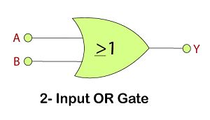
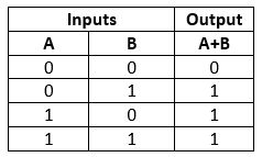
OR Gate
This gate works in the same way as the logical operator "OR". The OR gate is a circuit which performs the OR operation of the inputs.
Logic Design
Truth Table
NOT Gate
The NOT gate is also called an inverter. This gate gives the inverse value of the input value as a result.
Logic Design
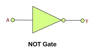
Truth Table
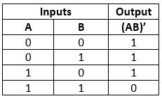
NAND Gate
The NAND gate is the combination of AND gate and NOT gate. This gate gives the same result as a NOT-AND operation.
Logic Design
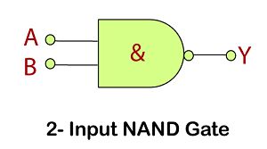
Truth Table
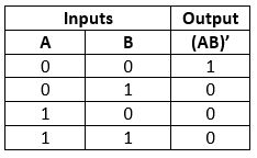
NOR Gate
The NOR gate is the combination of an OR gate and NOT gate. This gate gives the same result as the NOT-OR operation.
Logic Design
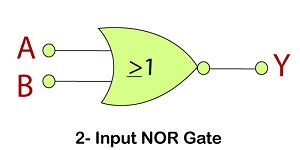
Truth Table
INTEGRATED CIRCUITS
(i) The concept of fabricating an entire circuit on a small single chip of semiconductor is called Integrated circuit; The chip dimensions are as small as 1mm * 1 mm or even less than that
(ii) The integrated chip can be categorised into (a) linear or analog IC (b) digital IC
(iii) Linear or Analog IC – The signals change continuously over a range of values between maximum and minimum; The output varies linearly as the input ; The most useful linear IC is an operational amplifier
(iv) DigitaIC – These have two values – high and low; These contain logical gates. – Depending upon the number of circuit components or logic gates used, they can be classified into SSI, MSI, LSI or VLSI